
 The Digital Age’s Key to Optimizing Your Entertainment Experience
  What Every Android User Should Know About com.wssyncmldm and Updates
  Android Services Library Keeps Stopping? Fix It Now!
  What is LPPe Service Android and How Does It Work? A Detailed Analysis
  How to Address the Unified Daemon Stopped Error on Samsung Devices
  Companion Device Manager: Pivotal Tool in Modern Tech
  TurboTax vs Keeper Tax: The Tech Frontier of Tax Solutions
  PowerSave Reviews: A Game-Changer in Energy Efficiency?
  How to Check Points at Walmart: Unleash the Power of Savvy Shopping with Samsung
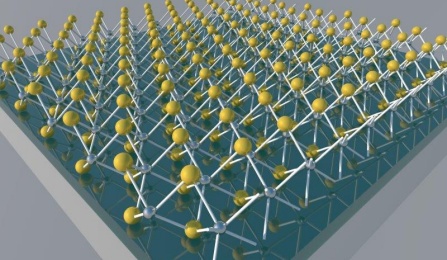
A Nanocavity can be considered as a nanometer scale structure that is used to trap light. The concentration of light in a small volume leads to an increase in the strength of the light. This can lead to an alteration of the spontaneous emission from the light source within the cavity.
Though the future of cinema and manufacturing industries might be 3D, but as far as photonics and electronics are concerned, things are going 2D especially the two dimensional semi-conductors. Recently, tests were carried out with a single layer of MoS2 (molybdenum disulphide) molecule that was placed over an optical Nanocavity (photonic structure).
What Exactly Is A Nanocavity?
The Nanocavity is typically made of aluminum, germanium and aluminum oxide. In the trials that have been conducted, light was passed through the germanium layer (1.50 – 3.00 nanometres thick) and circulated in a closed loop through the aluminum and the aluminum oxide.
It is being said that the Nanocavity developed so far has got a lot of potential. It has the potential with which flexible and efficient solar panels can be developed. These could also be used in making video cameras, faster photo detectors as well as other devices. It could also be used to split water more efficiently to produce hydrogen fuel. The band gap structure of a layer of molybdenum disulphide has an advantage as it is identical to the semi-conductors used in solar cells, lasers and LEDs.
What is the Current Status?
During the time of experiment, it was found that the Nanocavity could absorb up to 70% of the laser projected at it. This ability to absorb light to convert it into energy could be of help to come up with energy efficient electronic gadgets.
Researchers have commented that what they have found so far is just the surface of it. They are pretty hopeful with whatever work they might have done so far. They claim that further advancement can pave the way for major breakthroughs in this field of energy conversion and harvesting. It can also have implications in security systems and other important domains that will help mankind.
In electronics, semi-conductors form the base. They aid in manipulating the flow of energy in the devices. The widely known silicon is a semiconductor used in making microchips for computers, mobiles and many other electronic gadgets.
The Future Of Nano Cavity
The industry has always been on the look-out for thinner, smaller and more powerful opto-electronic devices. To achieve that, the size of the semi-conductor given in the devices contained was reduced. However, the issue with opto-electronic devices is that the ultra-thin semi-conductors are incapable of absorbing light as does the traditional bulk semi-conductors. Thus, there has always been a conflict between the thickness of the semi-conductor and its ability to absorb light or energy. The Nanocavity, on the other hand, is being looked at as a solution to this stand-off.
The electronic industry has always been on the hunt for micro-chips, but with higher capacity so that devices can be made more handy than before and with Nanocavity , things seem to be going in that direction.